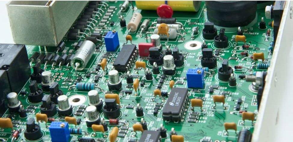
Historians have named several periods of the past by the material that typified the industry of the time, whether it be the Stone Age or Bronze Age or Iron Age. In keeping with that methodology our present period of history should then be called the Silicon Age. Computers and other electronic devices are everywhere nowadays, you carry your smartphone with you where ever you go but there are dozens of other electronic devices in your home as well. Your oven, washing machine, refrigerator even your car all have integrated circuits in them while of course your TV and computer are virtually nothing but Integrated Circuits made of silicon.
All of that is due to silicon’s properties as a ‘semi-conductor’ that is silicon is a material that doesn’t conduct electricity as well as a conducting metal, say copper or iron do, but it does conduct electricity better than an insulator like rubber or wood do. With all of the silicon electronics now being manufactured it’s rather surprising therefore to learn that silicon isn’t really all that good of a semi-conductor.
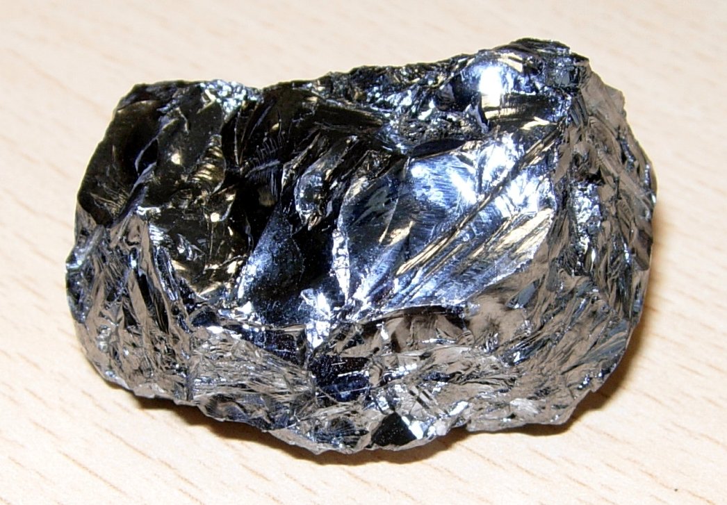
Silicon’s biggest problem is that while it does conduct electricity fairly well it is very bad at conducting heat away from the electronics. That’s why so many of our electronic devices get so hot, and require extra cooling systems to remove that heat before it reduces both the performance and lifespan of those electronics. Even as a semi-conductor however silicon is simply not as good as its rivals germanium (Ge) or gallium-arsenide (GaAs).
The primary factor of how good a semi-conductor material performs is called its carrier mobility, which is measured in units of centimeter-squared per volt second. There are actually two kinds of mobility, one for the electrons themselves called electron mobility and the other is ‘hole’ mobility, the mobility of places where an electron should be but isn’t. In a semiconductor a hole will actually behave like a positively charged electron. While the electron mobility of silicon is fairly good at 1400cm2/V*s, its hole mobility is much lower, only 450 cm2/V*s.

So why do we use silicon then? As you might guess cost is the major factor, germanium and gallium-arsenide are both considerably more expensive and gallium-arsenide is very toxic to boot, adding further to the cost of using it. Because of these drawbacks materials scientists are always on the lookout for new semi-conductor materials in the hope of finding a replacement for silicon.
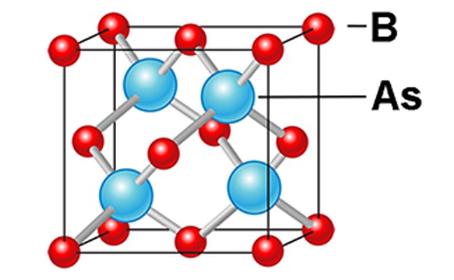
Now researchers at the University of Houston have identified a new semi-conductor material that not only surpasses silicon in performance but may actually approach the theoretical limit to semi-conductor performance. The material is called Cubic Boron-Arsenide (c-BAs for short) and is a crystal grown from the two elements Boron and Arsenic. To date only tiny crystals of c-BAs have been manufactured, and those have contained impurities, but recent measurements of c-BAs have shown that it possesses ten times the thermal conductivity of silicon while at the same time having a carrier mobility in excess of 1600 cm2/Vs for both electrons and holes. Based on their measurements the researchers also think that, if the impurities were removed, carrier mobility could reach as high as 3000 cm2/Vs.
Of course right now c-BAs is even more expensive than Ge or GaAs but to date very little research has been carried out to see if it can be manufactured on an industrial scale. If it can then c-BAs may become the new silicon, pushing the performance of electronics still further while improving their reliability and life span.
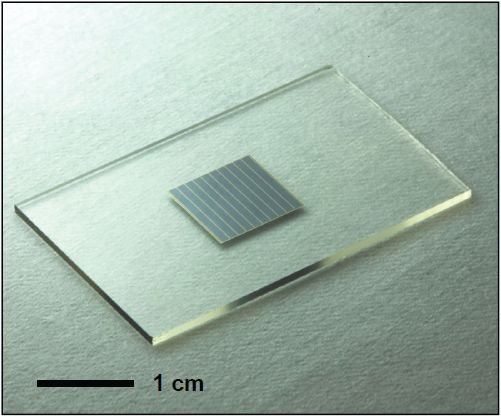
Ok, so what is it about these semiconductors that make them so valuable in electronics. To answer that question we first have to discuss the process of doping of a semiconductor. As I said above, semi-conductors will allow both electrons and electron holes to move through them, but not very well. If a very small amount of another element is mixed in however, about one atom of the other element for every 100 million atoms of silicon, that mobility can be greatly increased. For example adding that tiny amount of phosphorus to silicon increases its conductivity by a factor of 10,000.

This process is called doping and whether the increase is for electrons or holes depends on what material the silicon is doped with. Doping with phosphorus or antimony for example creates N-type silicon increasing the electron mobility. Doping with Boron or indium on the other hand results in P-type silicon with increased hole mobility. When a slice of N-type silicon is placed against a slice of P-type a semiconductor junction is formed where the free electrons can move into the holes but the holes cannot move into the electrons. In such a N-P junction electric current can only flow in one direction, a device known as a diode. Two such junctions, whether NPN or PNP form a transistor that can be switched ON or OFF or used to amplify a signal.
Semiconductor junctions can also both convert electric current to light, a Light Emitting Diode or LED, or convert light to electric current as in a solar cell. They can also convert heat to electricity or electricity to heat, that last part is easy. With all of its many applications it’s no wonder that materials scientists will continue to search for better, and cheaper semi-conductors.