Earlier this year I celebrated the fiftieth anniversary of the Moon landing of Apollo 11 by publishing a series of eight articles about the ‘Space Race’ of the 1960s. I enjoyed that task so much that I decided to write a few more posts about some of the other cool technologies of that time, I hope you enjoy them.
In most homes today you’ll find that the number of electronic devices outnumbers the number of human beings by a factor of three, four or even more. Add up all of the TVs, computers, smartphones, hey even our ovens and refrigerators have microprocessors in them nowadays!!! Electronics are so cheap, so versatile and so small that we’re putting them in just about everything.

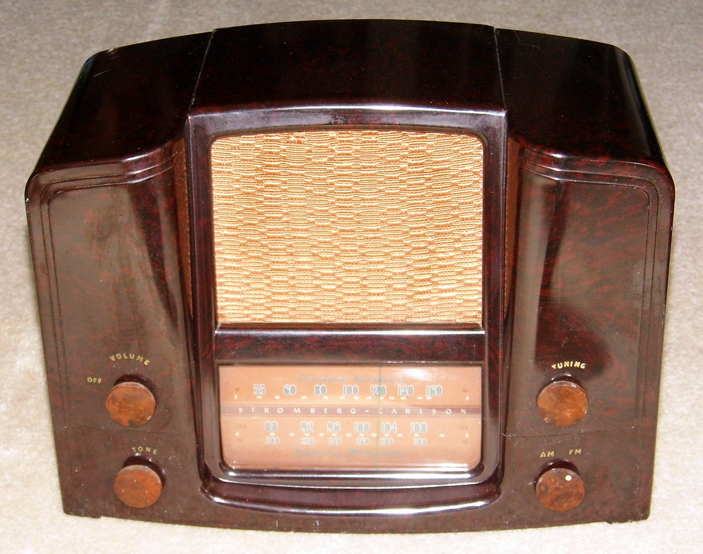
Back in the 60s however electronics were big and expensive. Most homes had one TV, one record player and one, maybe two radios. The reason was simple; electronics were built around the vacuum tube, which were themselves large and expensive. See image below.

Now if you think that a vacuum tube looks something like an incandescent light bulb you’re quite right, vacuum tubes were developed from light bulbs and like them require a considerable amount of power, voltage and current, in order to just turn on. This makes vacuum tubes wasteful of energy, hot and rather large.
Things started to change during the 60s when the first transistor electronics came on the market, the small, hand held AM transistor radio being the most popular. Now pretty much everyone knows that transistors are made primarily of silicon and, like a vacuum tube a transistor is an ultra fast electrical switch. Unlike a tube however a transistor doesn’t have to be hot in order to work.
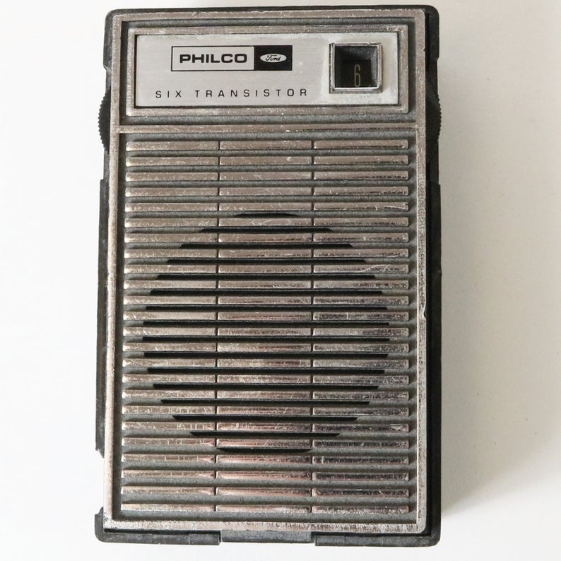
This means a transistor needs only a small fraction of the power of a vacuum tube in order to function and therefore they can be made much smaller and packed in together more tightly. Whereas a vacuum tube radio was as large as a piece of furniture a transistor radio could be held in one hand, and with the transistor radio the word miniaturization came into common usage.
Still, my first little transistor radio was build of ‘discrete’ transistors. That is to say each transistor was a separate object, an individual piece of silicon packaged in it’s own plastic coating. When I bought my second transistor radio I of course disassembled the first one and inside I found six transistors, along with numerous other components. The transistors were each about the size of a pea; I learned later that the transistors were packaged in a standard format known as TO-92.

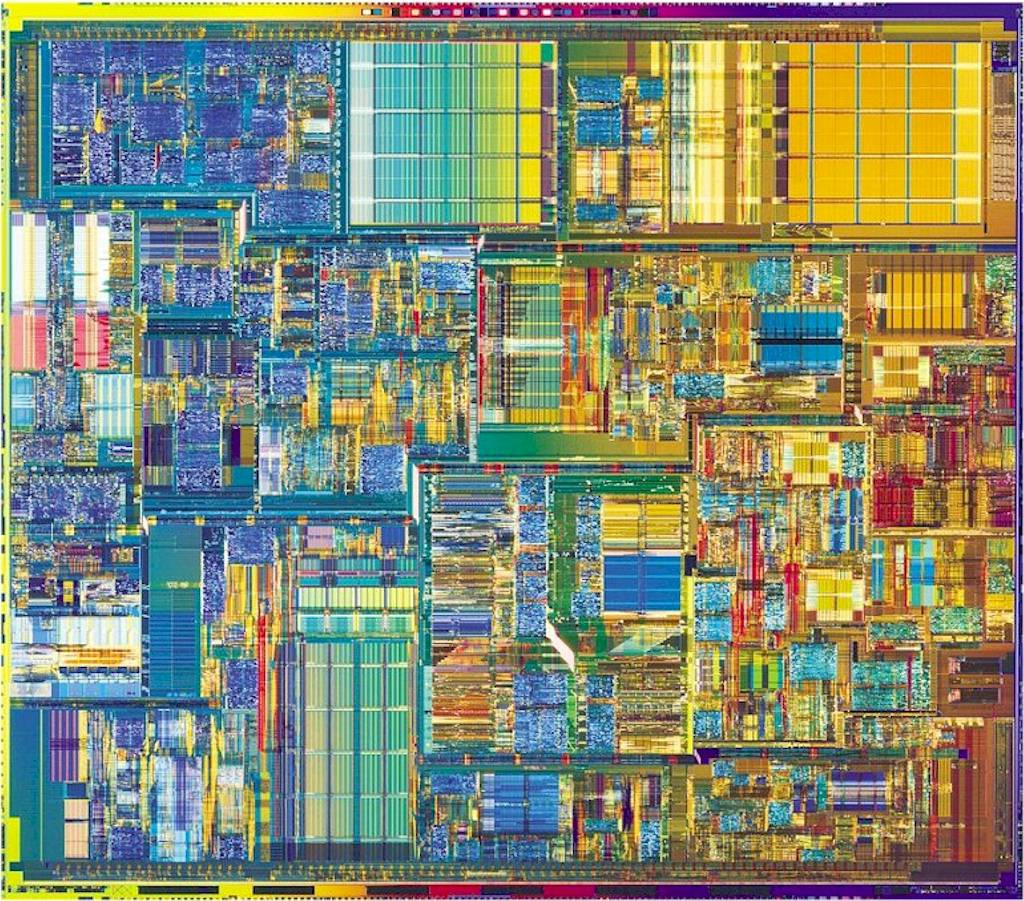
Even as the first transistorized consumer products were becoming available there were engineers who began to wonder if it would be possible to fit two transistors, or even more, on a single piece of silicon, and how many could you fit? The first experiments with Integrated Circuits (ICs), as these components came to be known, were carried out at Texas Instruments Corp. in 1958. See image below.

The advantages of ICs were many, reduced cost, size and power requirement along with increased operating speed. The drawback to ICs was their high initial start up costs. The facilities needed for manufacturing ICs, known as a ‘foundry’, are very expensive even though, once you had a foundry millions of ICs could then be made very cheaply. In the business this is known as a high Non-Recurring Expense (NRE) with a small Recurring Expense (RE).
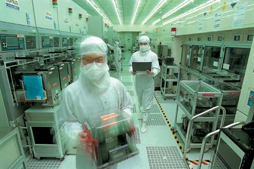
So, who was going to pay for the first IC foundries? The U.S. government that’s who! In the 1960s both NASA and the military had a tremendous need for ever more sophisticated radios, radars, guidance systems and even computers. And all of these new electronics had to be smaller in order to fit into rockets, airplanes and ships. The IC was the only possible technology that could satisfy that need.
Then, once the first foundries were built the miniaturization revolution really got under way. One of the pioneers of the IC industry Gordon Moore declared in 1965 that the number of transistors on a single silicon ‘chip’ would double ever two years. This prediction is commonly called Moore’s Law and has worked now for over 50 years with the current technology being capable of placing millions of transistors on a chip of silicon no larger than a fingernail.

With this technological progress has come personal computers, smartphones, digital cameras, digital television and myriad other devices that we all have in our homes or carry on our person. The transistor and Integrated Circuit have become the true symbols of our modern age and their revolution began in the 1960s.